
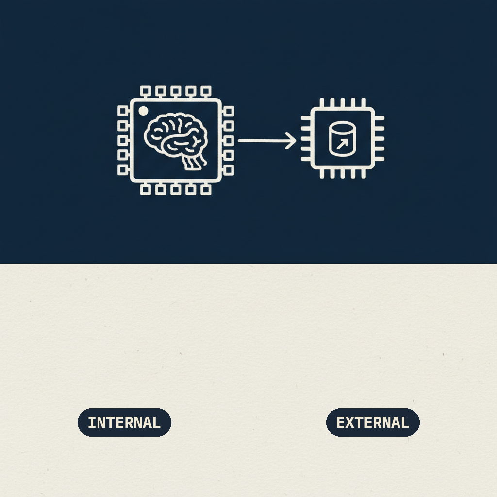
I want to write about a risk assessment I did recently, and I want to be careful to keep it framed as exactly that: an assessment, not a result. This is not a "we built it and it works" post. It's a "here's why I feel meaningfully better about this approach than I did a week ago, and here's precisely what still needs to be proven" post.
The problem we're evaluating
Our nRF54L15 mesh firmware needs an OTA update mechanism, and MCUboot is the natural choice — it's the standard bootloader in the Zephyr/nRF Connect SDK ecosystem, and we're already leaning on that ecosystem elsewhere. The open question was whether we could put MCUboot's secondary OTA slot — the "staging area" an update image lands in before it gets swapped into the primary slot — on external flash rather than the chip's internal flash. Given how tight our internal flash budget already is (a topic for another post), moving the secondary slot off-chip is an attractive way to buy back headroom for the image that actually runs.
The catch is that external flash for a secondary slot isn't a trivial bolt-on. It touches how MCUboot addresses storage, how the image gets written and verified, and how the swap actually happens at boot. This is exactly the kind of thing where "should work in theory" and "works" can diverge, so before committing engineering time to it, I wanted to understand how much of this Nordic had already solved for us versus how much we'd be building from scratch.
What changed my assessment
I spent time going through the nRF Connect SDK source rather than just relying on documentation summaries, and what I found was better than I expected. Nordic officially ships a reference overlay for exactly this configuration — an external flash secondary slot, specifically for the nRF54L15 DK. This isn't a community workaround or a stale example that's bitrotted since some SDK version bump; it's an overlay Nordic maintains as part of their own reference material for this chip.
That matters a lot for risk assessment. It means the wiring between MCUboot's slot configuration and external flash addressing has already been thought through by the people who wrote MCUboot's Zephyr integration, not something we'd be reverse-engineering from partial documentation. And practically, it means we have a known-good starting point to diff our own configuration against if something doesn't behave the way we expect.
The other piece of good news: the nRF54L15 DK has external flash built onto the board already. For prototyping this, that means no extra wiring, no breakout board, no soldering a flash chip onto a dev kit before we can even start testing. We can point the reference overlay at hardware we already have on the bench.
What I have not done, and want to be explicit about
I have not built this firmware with the external flash overlay applied. I have not flashed it onto a DK. I have not performed an actual OTA update that writes an image into the external secondary slot and triggers MCUboot to swap it into the primary slot. In other words, the entire "does the swap actually happen correctly, does verification pass, does the device boot the new image" question is still untested. Reading source code lowers my estimate of how likely we are to hit a nasty surprise; it doesn't replace actually hitting the surprise or not.
So where does that leave things? Genuinely more optimistic than I was — going from "this might require significant custom bootloader work" to "this looks like configuration on top of a supported reference design" is a real shift. But the next concrete step is unambiguous: build it, flash it, and run an actual OTA slot-swap test on the DK. Until that happens, this stays a risk assessment, not a result, and I'd rather say that plainly than let cautious optimism quietly turn into an unearned claim of "it works."
想寫寫我最近做的一次風險評估,而且想很小心地把它框在「評估」這個範疇裡,不多不少:這不是一篇「我們做出來了、能動」的文章。這是一篇「跟一週前比,我現在對這個做法的信心明顯提升了,以下是原因,以及具體還有哪些事還沒被證實」的文章。
我們在評估的問題
我們的 nRF54L15 mesh 韌體需要一套 OTA 更新機制,而 MCUboot 是很自然的選擇——它是 Zephyr/nRF Connect SDK 生態系裡的標準 bootloader,而我們在其他地方也已經在依賴這套生態系。懸而未決的問題是:能不能把 MCUboot 的 secondary OTA slot——也就是更新映像檔在被 swap 進 primary slot 之前的「暫存區」——放到外部 flash,而不是晶片內建的 internal flash 上。考慮到我們內部 flash 預算已經多緊(這是另一篇文章的主題),把 secondary slot 搬到晶片外,是為真正在跑的映像檔買回一些餘裕空間的誘人做法。
問題在於,外部 flash 當 secondary slot 不是隨便接上就能用的小事。它牽涉到 MCUboot 怎麼定址儲存空間、映像檔怎麼寫入跟驗證、以及開機時 swap 實際上是怎麼發生的。這正是「理論上應該可行」跟「真的可行」很容易分岔的地方,所以在投入工程時間之前,我想先搞清楚 Nordic 已經幫我們解決了多少,又有多少得從零開始自己搭。
是什麼改變了我的評估
我花時間直接讀 nRF Connect SDK 的原始碼,而不是只看文件摘要,結果比我預期的好。Nordic 官方就直接提供了針對這個確切配置的參考 overlay——外部 flash secondary slot,而且specifically 就是給 nRF54L15 DK 用的。這不是社群拼湊出來的 workaround,也不是隨著某次 SDK 版本升級就爛掉的舊範例;這是 Nordic 自己維護、作為這顆晶片官方參考資料一部分的 overlay。
這對風險評估來說意義很大。代表 MCUboot slot 配置跟外部 flash 定址之間的接線,已經被寫 MCUboot Zephyr 整合層的人想清楚過了,不是我們得從殘缺文件裡逆向工程出來的東西。實務上,這也代表萬一我們自己的配置跑起來不如預期,我們有一個已知能動的起點可以拿來 diff。
另一個好消息是:nRF54L15 DK 板子上本身就內建外部 flash。這對做 prototype 來說,代表不用額外接線、不用外接子板、不用在能開始測試之前先把一顆 flash 晶片焊到 dev kit 上。我們可以直接把參考 overlay 套用到手邊現成的硬體上。
我還沒做的事,想講清楚
我還沒有把外部 flash overlay 套上去、真的 build 出這套韌體。我還沒有把它燒進 DK。我還沒有真正執行過一次 OTA 更新——把映像檔寫進外部的 secondary slot、觸發 MCUboot 把它 swap 進 primary slot。換句話說,「swap 到底有沒有正確發生、驗證有沒有通過、裝置有沒有真的開機跑起新映像檔」這整個問題,都還沒被測試過。讀原始碼降低了我們踩到討厭意外的機率估計,但它取代不了真的去踩、或確認不會踩到這個過程本身。
所以現在的狀態是什麼?老實說,比之前樂觀不少——從「這可能需要大量客製化 bootloader 工作」變成「這看起來只是在一個有官方支援的參考設計上做配置」,是個真實的轉變。但接下來具體要做的事很明確:build 出來、燒進去,在 DK 上跑一次真正的 OTA slot-swap 測試。在那之前,這件事的定位就是風險評估,不是結果,我寧可直白地這樣講,也不想讓謹慎的樂觀悄悄變成一句站不住腳的「它能動」。